- 您现在的位置:买卖IC网 > Sheet目录318 > CAT4008W-T2 (ON Semiconductor)IC LED DRIVER LINEAR 16-SOIC
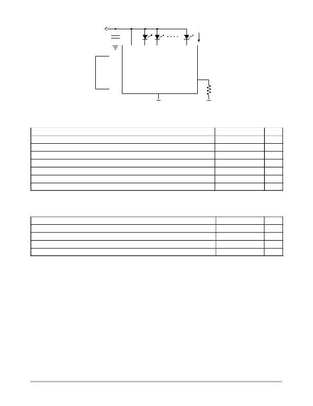
CAT4008
VIN
3 V to
5.5 V
1 m F
VDD LED1 LED2
LED8
20 mA
BLANK
LATCH
CAT4008
SOUT
to next
device
SIN
CLK
GND
RSET
3.09 k W
Figure 1. Typical Application Circuit
Table 1. ABSOLUTE MAXIMUM RATINGS
Parameter
V DD Supply Voltage
Logic input/output voltage (SIN, SOUT, CLK, BLANK, LATCH)
LEDn voltage
DC output current on LED1 to LED8
Storage Temperature Range
Junction Temperature Range
Lead Soldering Temperature (10 sec.)
Rating
6
? 0.3 V to V DD +0.3 V
6
150
? 55 to +160
? 40 to +150
300
Units
V
V
V
mA
_ C
_ C
_ C
Stresses exceeding Maximum Ratings may damage the device. Maximum Ratings are stress ratings only. Functional operation above the
Recommended Operating Conditions is not implied. Extended exposure to stresses above the Recommended Operating Conditions may affect
device reliability.
Table 2. RECOMMENDED OPERATING CONDITIONS
V DD
Voltage applied to LED1 to LED8
LED current RSET control range
Ambient Temperature Range
Parameter
http://onsemi.com
2
Range
3.0 to 5.5
0.4 to 5.5
up to 100
? 40 to +85
Units
V
V
mA
_ C
发布紧急采购,3分钟左右您将得到回复。
相关PDF资料
CAT4101TV-T75
IC LED DRVR HP CONST CURR D2PAK
CAT4104V-GT3
IC LED DVR 4CH 175MA 8SOIC
CAT4106YP-T2
IC LED DVR 4CH BOOST 16TSSOP
CAT4109V-GT2
IC LED DRIVER RGB 16-SOIC
CAT4134HV2-T2
IC LED DRVR BKLGHT FLASH 12-TDFN
CAT4137TD-T3
IC LED DRVR WHITE BCKLGHT TSOT-5
CAT4139TD-GT3
IC LED DRVR WHITE BCKLGT TSOT-5
CAT4237TD-T3
IC LED DRVR WHITE BCKLGHT TSOT-5
相关代理商/技术参数
CAT4008Y
制造商:Rochester Electronics LLC 功能描述: 制造商:Catalyst Semiconductor 功能描述:
CAT4008Y-GT2
制造商:ONSEMI 制造商全称:ON Semiconductor 功能描述:8-Channel Constant Current LED Driver
CAT4008Y-T2
功能描述:LED照明驱动器 LED Driver 8 Chan 4-wire I/F RoHS:否 制造商:STMicroelectronics 输入电压:11.5 V to 23 V 工作频率: 最大电源电流:1.7 mA 输出电流: 最大工作温度: 安装风格:SMD/SMT 封装 / 箱体:SO-16N
CAT4016
制造商:ONSEMI 制造商全称:ON Semiconductor 功能描述:16-Channel Constant Current LED Driver
CAT4016_08
制造商:CATALYST 制造商全称:Catalyst Semiconductor 功能描述:16-Channel Constant Current LED Driver
CAT4016HV6
制造商:Rochester Electronics LLC 功能描述: 制造商:Catalyst Semiconductor 功能描述:
CAT4016HV6G
制造商:Rochester Electronics LLC 功能描述: 制造商:Catalyst Semiconductor 功能描述:
CAT4016HV6-GT2
功能描述:LED照明驱动器 LED Driver,16 Chan 4-wire I/F RoHS:否 制造商:STMicroelectronics 输入电压:11.5 V to 23 V 工作频率: 最大电源电流:1.7 mA 输出电流: 最大工作温度: 安装风格:SMD/SMT 封装 / 箱体:SO-16N
